-
 Hitachi SEM Pics
Started in this thread:
http://www.photonlexicon.com/forums/...-a-Hitachi-SEM
Got the EDX running, EDX allows you to do elemental analysis by sampling the x-rays that are created when the electron beam hits the target in the microscope.
I picked up a 50L dewar of liquid nitrogen last Monday and filled the dewar on the EDX head. You need to let it sit from 4-10 hours to make sure the sensor is cooled. If the sensor is not cool (cryogenic temps) the sensor will be ruined.
I calibrated the EDX a few nights ago, the software uses a sample with aluminum and copper to create a spectrum and then figures out the offset and gain to get the peaks in the right place. With that done I zoomed into the little screw in the picture with the dime edge and did an acquisition. This is what I got and the analysis side says the screw is composed of the following:
Element Line Weight% K-Ratio Cnts/s Atomic%
---------------------------------------------------------
Al Ka 6.26 0.0115 90.84 13.78
Fe Ka 1.68 0.0206 77.55 1.79
Ni Ka 1.06 0.0130 39.00 1.08
Cu Ka 55.95 0.5566 1483.97 52.35
Zn Ka 31.62 0.3132 728.50 28.76
Sr La 1.91 0.0066 19.13 1.30
Mo La 1.51 0.0079 23.45 0.94
Total 99.99
This works out to be a brass with aluminum added. Adding aluminum increases the strength of brass and makes it more corrosion resistant.
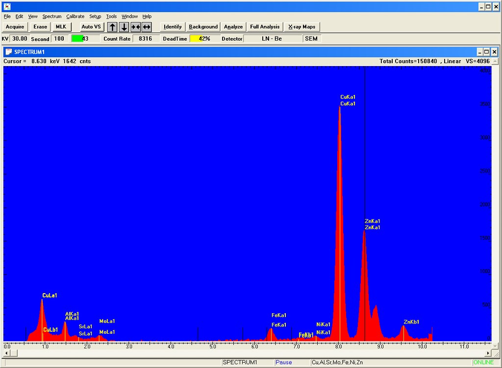 screwspectrum by macona, on Flickr
I threw a piece if U Ore in the scope to see what it would show, here it is:
[A N A L Y S I S R E P O R T]
GENERAL CONDITIONS
------------------
Result File : UORE
File Version : 1
Background Method : Foil
Decon Method : Gaussian
Decon ChiSquared : 6.13
Analysis Date : 28-DEC-2014
Microscope : SEM
Comments :
ANALYSIS CONDITIONS
-------------------
Quant. Method : XPP/ASAP
Acquire Time : 400 secs
Normalization Factor: 100.00
SAMPLE CONDITIONS
-----------------
kV : 30.0
Beam Current : 100.0 picoAmps
Working Distance : 25.0 mm
Tilt Angle : 30.0 Degrees
TakeOff Angle : 35.0 Degrees
Solid Angle*BeamCurrent: 0.9
Element Line Weight% K-Ratio Cnts/s Atomic%
---------------------------------------------------------
Mg Ka 3.16 0.0117 9.87 5.37
Al Ka 8.21 0.0365 33.43 12.59
Si Ka 40.97 0.2064 194.23 60.36
Ca Ka 7.39 0.0471 33.73 7.63
Ti Ka 0.00 0.0000 0.00 0.00
Fe Ka 8.69 0.0743 32.49 6.44
Cu Ka 3.47 0.0309 9.58 2.26
Pd La 0.00 0.0000 0.00 0.00
Au La 12.69 0.1014 8.26 2.67
U La 15.42 0.1138 2.89 2.68
Total 100.00
I was surprised by the gold. I guess I should have not been, U was first found in Gold mines so says the internets. But I am scanning a very tiny piece of the ore so who knows if it is homogenous throughout the sample.
 UOre by macona, on Flickr
Not really, there is not enough beta emission to activate the phosphor on the secondary electron detector (I tried) and the gamma energies are higher than the x-ray detector does.
Tried the Map mode of the EDX for the first time last night. In the center window you can see an image of the sample (U Ore) and the surrounding images are heat maps of different elements that are found in that image. the more towards the red end of the spectrum, the more of that element was found. This was a "quick" 256x256 scan at 15ms per pixel dwell time. It took 15 minutes. Looks like it is a very time consuming process but still pretty neat.
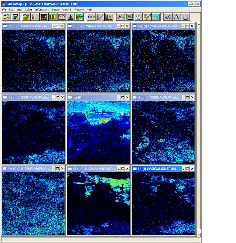 uoremap by macona, on Flickr
I analyzed a piece of goldish metal that came out of a machine that was used for washing silicon wafers. It is 81% gold, 11% rubidium, 3% Iron, and the rest copper. I was not expecting to find this in the flake, this is at 490x.
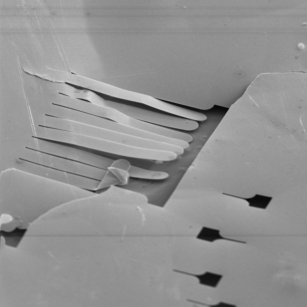 GOLDFLAE by macona, on Flickr
-
From estimation that "big" feature in the pic above is about 5um across.
-
that's a brush with little 'holes' shaped perfectly to allow a slurry of fluid between the brushes and wafer?
-
No, my guess is that this material is what comes off the area coated with photoresist. The parts missing are left on the wafer as contacts or connections, maybe gates from a mosfet or something.
-
Cool pics!
OK, now I have another item to add to my bucket-list of toys. Scanning Electron Microscope! Sigh... Wonder if my wife would let me put it in the dining room?
Adam
-
... if not SEM, then AFM - this 'toys' can be smaller than a shoe-carton and have resolutions down to single nanometers, even with a DIY-thingy made with three bulk piezo-blocks ... and you won't need vacuum ;-)
Viktor
-
The pictures you get from an atomic force microscope are not as impressive as the ones from a scanning electron microscope, at least in my opinion. Yeah, I know the AFM has a greater resolution.... But there's a "coolness" factor in the images you get from a SEM. (Check out these other images that macona posted in this earlier thread.)
Adam
-
... yes, mostly - see the SEM-image in my post #12 here - http://www.photonlexicon.com/forums/...light=nailhead
But an AFM can be used with a much bigger scale than 'atomic' - it's as simple as sticking three piezo-actors together and scan/sample with a height-sensor a non uniform surface or even small objects on a surface.
Here some links for DIY-AFM's:
- with sample images -- http://www.instructables.com/id/A-DIY-AFM-Whokshop/
- here a more scintific based one -- http://web.archive.org/web/200801061...de/PlasticAFM/
Viktor

 Posting Permissions
- You may not post new threads
- You may not post replies
- You may not post attachments
- You may not edit your posts
-
Forum Rules


 Reply With Quote
 buffo
buffo